Developed by SECO/WARWICK – one of the world’s leading manufacturers of heat processing equipment and a technology leader
With our fully equipped research and development facility and cooperation with the academic centers in Europe, we are able to provide innovative solutions not ofered anywhere else in the world. The Group is made up of companies located in five countries on three continents, and We sell our products Worldwide. We supply our equipment to customers involved in steel, titanium and aluminum production as well as aluminum recycling, forging, automotive, aerospace, commercial heat treating, HVAC/R, electronics, Wind energy, medical equipment and nuclear industries.
For wide range of industrial and R&D applications
- Working temperature up to 1200°C
- Substrate formats up to 500 x 500 mm (larger reactors on request)
- Ability to load multiple levels of substrate in one batch
- Growth ofgraphene on 3d objects
- Flexible control system and intuitive HM
Flexible equipment
- Large formats and/or small samples can be processed
- Different gasses and mixtures can be used
- Process can be conducted in vacuum / partial pressure and positive pressure (from 10′; Torr to 1,5 bar absi)
- Variable process temperature and heat-up rate
- Variable cooling rate in vacuum, still atmosphere or accelerated atmosphere
FIND OUT MORE: https://www.secowarwick.com/en/purification-of-graphite-materials/
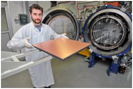 High quality CVD graphene in formats up to 500 x 500 mm
|
 Optical microscope image of graphene layer grown on Cu foil, transferred on to SiO2 substrate shows continuous layer without cracks, holes, etc.
|
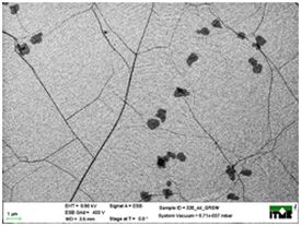 SEM (Scanning Electron Microscope) image confirms no macro-defects in the graphene layers. Very few of the second graphene layer seeds (dark islands). |
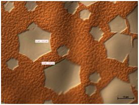 Graphene domains size up to 0.1 mm |
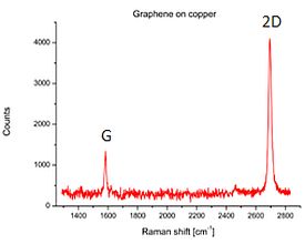 Raman spectrum confirms the high quality of graphene layer grown on copper. No observable D (defective) peak. Small FWHM of 2D peak indicates a true single layer of graphene |
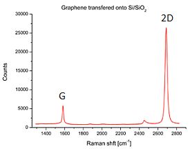 Raman spectrum of high quality graphene grown on Cu foil and transferred on to SiO2 substrate. Small FWHM of 2D peak indicates a true single layer of graphene; D peak is not observed, which indicates low defects level. |
Electrical parameters have been measured based on Hall effect in Van der Pauw configuration at RT over 1cm x 1cm samples of graphene transferred onto Si/SiO2 substrate.
- high carrier concentration:
p= 1,257E13
µ= 1148
ρ= 433
- low carrier concentration:
p= 2.393E12
µ= 1771
ρ= 1476
where:
p- sheet hole concentration [cm-2]
µ- carrier mobility [cm2/V·s]
ρ- resistivity [Ω·cm]